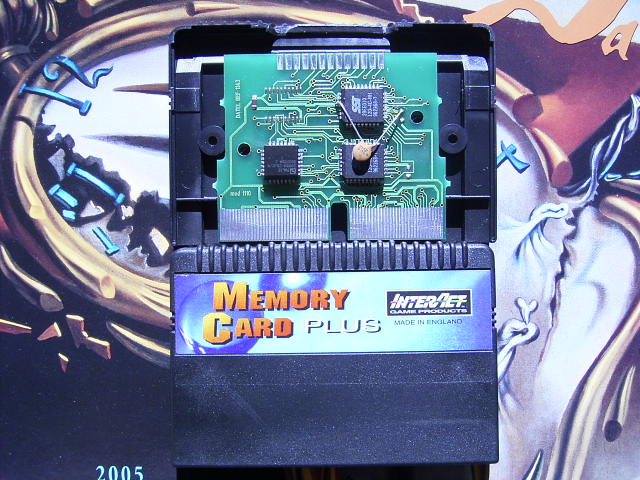
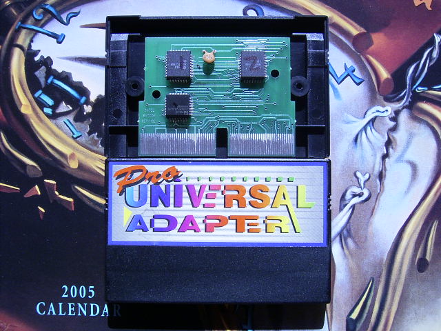
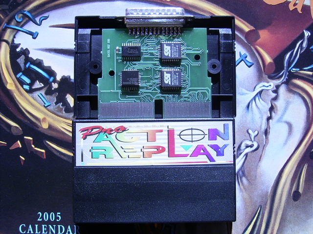
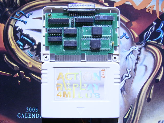
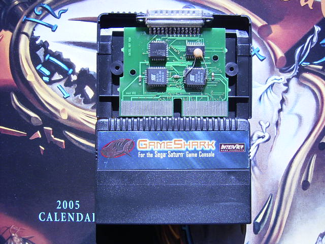
cartridge
front
(right to left)
(component side)
|
pin
|
cartridge
back
(left to right)
(solder side)
|
VDD
5V
|
---
0 ---
|
VDD
5V |
|
---
1 ---
|
_A45 -> SMPC IC9 pin 4
|
GND
|
---
2 ---
|
VSS
|
VSS
|
---
3 ---
|
VSS
|
| D4
R / CPU D12 |
---
4 --- |
D3
R / CPU D11 |
| D5
R / CPU D13 |
---
5 --- |
D2
R / CPU D10 |
| D6
R / CPU D14 |
---
6 --- |
D1
R / CPU D9 |
| D7
R / CPU D15 |
---
7 --- |
D0
R / CPU D8 |
VSS
|
---
8 --- |
VSS
|
| D4
L / CPU D4 |
---
9 --- |
D3
L / CPU D3 |
| D5
L / CPU D5 |
---
10 --- |
D2
L / CPU D2 |
| D6
L / CPU D6 |
---
11 --- |
D1
L / CPU D1 |
| D7
L / CPU D7 |
---
12 --- |
D0
L / MCP: 20V8H pin 19(I/O 1) / CPU
D0 |
VSS
|
---
13 --- |
VSS
|
|
---
14 --- |
|
|
---
15 --- |
PAR: 22V10 pin 10
|
PAR: 22V10 pin 7
|
---
16 --- |
|
PAR: 22V10 pin 6
|
---
17 --- |
|
CLK
(ATF16V8B I/CLK 1) PAR: 16V8 pin 1
|
---
18 --- |
PUA:
20V8H pin 5(I 3) / PAR: Flash
memory /WE
|
MCP:
20V8H pin 27(I 13) / PAR: 16V8 pin
12
|
---
19 --- |
|
KOF: ROM /OE, PAR: 22V10 pin 3
|
---
20 --- |
KOF: ROM /CE, PAR: 22V10 pin 2
|
VSS
|
---
21 --- |
VSS
|
|
---
22 --- |
A0
/ CPU A0 |
| A1
/ CPU A1 |
---
23 --- |
A9
/ CPU A9 |
| A2
/ CPU A2 |
---
24 --- |
A10
/ CPU A10 |
| A3
/ CPU A3 |
---
25 --- |
A8
/ CPU A8 |
VSS
|
---
26 --- |
VSS
|
| A4
/ CPU A4 |
---
27 --- |
A7
/ CPU A7 |
| A5
/ CPU A5 |
---
28 --- |
A12
/ CPU A12 |
| A6
/ CPU A6 |
---
29 --- |
A11
/ CPU A11 |
A13
/ CPU A13
|
---
30 --- |
A14
/ CPU A14 |
|
------
|
|
|
------
|
|
|
------
|
|
|
------
|
|
VSS
|
---
31 --- |
VSS
|
| A15
/ CPU A15 |
---
32 ---
|
A16
/ CPU A16 |
| /
CPU A17 |
---
33 --- |
MCP:
20V8H pin 4(I 2) / CPU A18 |
| MCP:
20V8H pin 11(I 8) / CPU A19/ PAR:
PAL16V8 pin 7 |
---
34 --- |
PAR: 16V8 pin 6
|
EMS:
ATF16V8B pin 11 I9/ OE,
MCP:
20V8H pin 17(I 12)
PAR: PAL16V8
pin 11 |
---
35 --- |
PAR: 16V8 pin 2
|
MCP:
20V8H pin 12(I 9) / PAR: PAL16V8
pin 8
|
---
36 --- |
PAR: 16V8 pin 5
|
|
---
37 --- |
VSS
|
VSS
|
---
38 --- |
VSS
|
|
---
39 --- |
|
| VDD
5V |
---
40 --- |
VCC
|
|
---
41 --- |
|
|
---
42 --- |
|
|
---
43 --- |
|
VSS
|
---
44 --- |
VSS
|
|
---
45 --- |
|
|
---
46 --- |
|
|
---
47 --- |
|
|
---
48 --- |
|
VSS
|
---
49 --- |
VSS
|
|
---
50 --- |
|
|
---
51 --- |
|
|
---
52 --- |
|
|
---
53 --- |
|
VSS
|
---
54 --- |
VSS
|
|
---
55 --- |
|
|
---
56 --- |
|
|
---
57 --- |
|
|
---
58 --- |
|
VSS
|
---
59 --- |
VSS
|
|
---
60 --- |
|
DS_WS
|
---
61 --- |
|
DS_CLOCK
|
---
62 --- |
|
DS_DATA
|
---
63 --- |
|
|
---
64 --- |
|
VDD
5V
|
---
65 --- |
VDD
5V |
VDD 5V
|
--- 66 --- |
VDD 5V |